Address
B-61, GIDC, Electronics Estate, Sector 25, Gandhinagar-382028, Gujarat, India.

Email
info.chetumaxsales@gmail.com

Mobile
+91 8490802084 
+91 9327083092

Work Hours
Monday to Friday: 9 AM - 7 PM

Matching CCL to the PCB Project – Perfect match for your needs

Matching CCL to the PCB Project - Perfect match for your needs
CCL Matching for your PCB Project needs

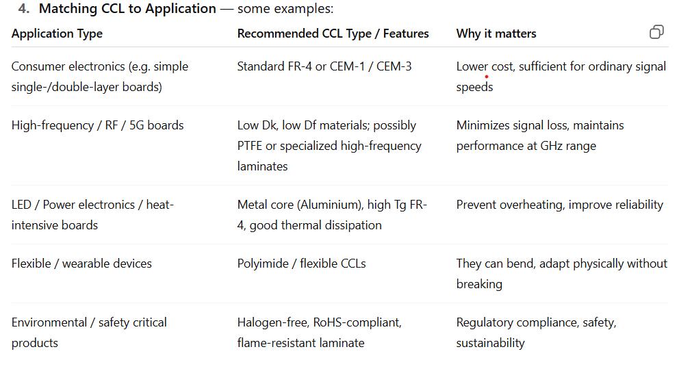
Sections / Key Points:

1.What is CCL and why it’s the base of PCB performance

A Copper Clad Laminate (CCL) is a basic material used to make printed circuit boards (PCBs), consisting of a thin sheet of copper foil bonded to an insulating core, like a fiberglass-reinforced epoxy resin. These laminates provide the necessary electrical insulation and mechanical support for circuits, and are processed to create the conductive pathways on a PCB. 

2.Types of CCL Materials / Substrates

  • FR-4 (standard, high Tg variant)
  • Halogen-free FR-4
  • Polyimide (for high temp, flexible)
  • Metal core / Aluminium CCL (for thermal dissipation)
  • CEM-1, CEM-3, paper-based (“cheap boards”)

3.Key Properties to Consider

  • Dielectric Constant (Dk) & Loss Tangent (Df) — especially for high frequency boards.
  • Thermal Properties: Tg (Glass transition), CTE (thermal expansion), thermal conductivity.
  • Mechanical Strength, Peel Strength (copper adhesion) etc.
  • Environmental / Regulatory: RoHS, Halogen-free, lead-free compatibility.

4.Cost vs Performance Trade-Offs

  • Why very high performance laminates cost more (raw material, special processes).
  • How sometimes over-spec’ing raises cost without benefit.
  • Suggestions how to optimize: pick the minimal spec that ensures lifetime and reliability, avoid unnecessary overengineering.

How Chetumax Sales and MM Enterprise assist you in choosing according to your needs:

  • Expertise in sourcing different types of CCL.
  • Help customers pick the correct spec.
  • Transparent quoting with explanation of material, copper weight, finish, etc, along with the option of importing at Chinese FOB price and if you want, we can import under your company name too.
  • Access to top-notch Chinese suppliers, with quality checks and certificates from SGS, RoHS so you don’t get surprises.
Step 1

Design and Output

Step 2

From File to Film

Step 3

Printing the Inner layers

Step 4

Removing the Unwanted Copper

Step 5

Layer Alignment and Optical Inspection

Step 6

Layer-up and Bond

Step 7

PCB Drill

Step 8

Plating and Copper Deposition

Step 9

Outer Layer Imaging

Step 10

Plating

Step 11

Final Etching

Step 12

Solder Mask Application

Step 13

Surface Finish

Step 14

Silkscreen

Step 15

Electrical Test

Step 16

Profiling and V-Scoring

Step 1:

Design and Output

  • Circuit boards should be rigorously compatible with, a PCB layout created by the designer using PCB design software. Commonly-used PCB design software includes Altium Designer, OrCAD, Pads, KiCad, Eagle etc. NOTE: Before PCB fabrication, designers should inform their contract manufacturer about the PCB design software version used to design the circuit since it helps avoid issues caused by discrepancies.
  • Once the PCB design is approved for production, designers export the design into format their manufacturers support. The PCB industry birthed extended Gerber as the perfect output format. Different PCB design software possibly calls for different Gerber file generation steps, they all encode comprehensive vital information including copper tracking layers, drill drawing, apertures, component notations and other options.

Leave a Reply

Your email address will not be published. Required fields are marked *